CD54HC299
CD54HC299 is 8-Bit Universal Shift Register manufactured by Texas Instruments.
Features
- Buffered Inputs
- Four Operating Modes: Shift Left, Shift Right, Load and Store
- Can be Cascaded for N-Bit Word Lengths
- I/O0
- I/O7 Bus Drive Capability and Three-State for Bus Oriented Applications
- Typical f MAX = 50MHz at VCC = 5V, CL = 15p F, TA = 25o C
- Fanout (Over Temperature Range)
- Standard Outputs
- -
- 10 LSTTL Loads
- Bus Driver Outputs
- - . . . 15 LSTTL Loads
- Wide Operating Temperature Range . . . -55o C to 125o C
- Balanced Propagation Delay and Transition Times
- Significant Power Reduction pared to LSTTL Logic ICs
- HC Types
- 2V to 6V Operation
- High Noise Immunity: NIL = 30%, NIH = 30% of VCC at VCC = 5V
- HCT Types
- 4.5V to 5.5V Operation
- Direct LSTTL Input Logic patibility, VIL= 0.8V (Max), VIH = 2V (Min)
- CMOS Input patibility, Il ≤ 1µA at VOL, VOH
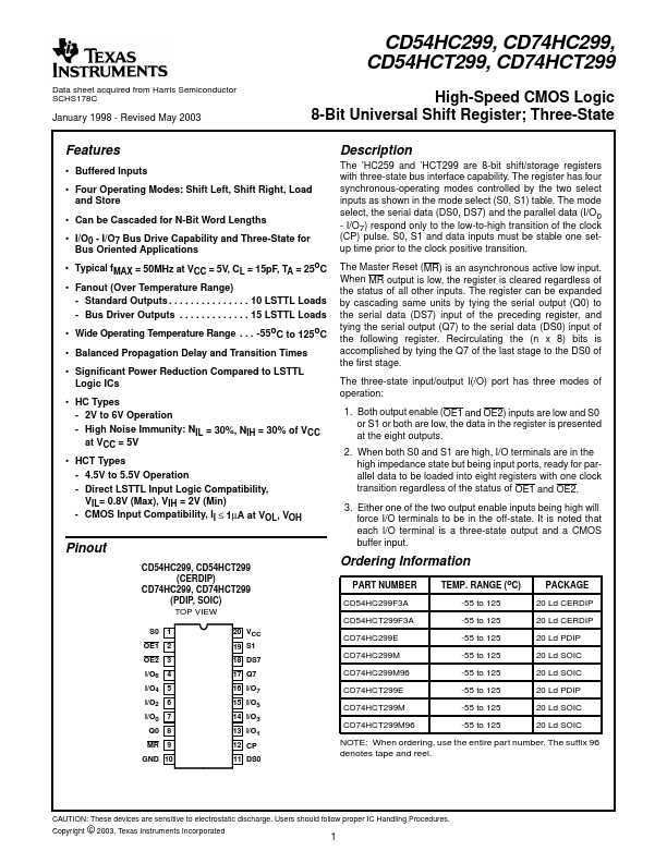
Pinout
CD54HC299, CD54HCT299 (CERDIP)
CD74HC299, CD74HCT299 (PDIP, SOIC) TOP VIEW
S0 1 OE1 2 OE2 3 I/O6 4 I/O4 5 I/O2 6 I/O0 7
Q0 8 MR 9 GND 10
20 VCC 19 S1 18 DS7 17 Q7 16 I/O7 15 I/O5 14 I/O3 13 I/O1 12 CP 11 DS0
Description
The ’HC259 and ’HCT299 are 8-bit shift/storage registers with three-state bus interface capability. The register has four synchronous-operating modes controlled by the two select inputs as shown in the mode select (S0, S1) table. The mode select, the serial data (DS0, DS7) and the parallel data (I/O0
- I/O7) respond only to the low-to-high transition of the clock (CP) pulse. S0, S1 and data inputs must be stable one setup time prior to the clock positive transition.
The Master Reset (MR) is an asynchronous active low input. When MR output is low, the register is cleared regardless of the status of all other inputs. The register can be expanded by cascading same units by tying the serial output (Q0) to the serial data (DS7) input of the preceding register, and tying the serial output (Q7) to the serial data (DS0) input of the following register. Recirculating the (n x 8) bits is acplished by tying the Q7 of the last...